Skip to content

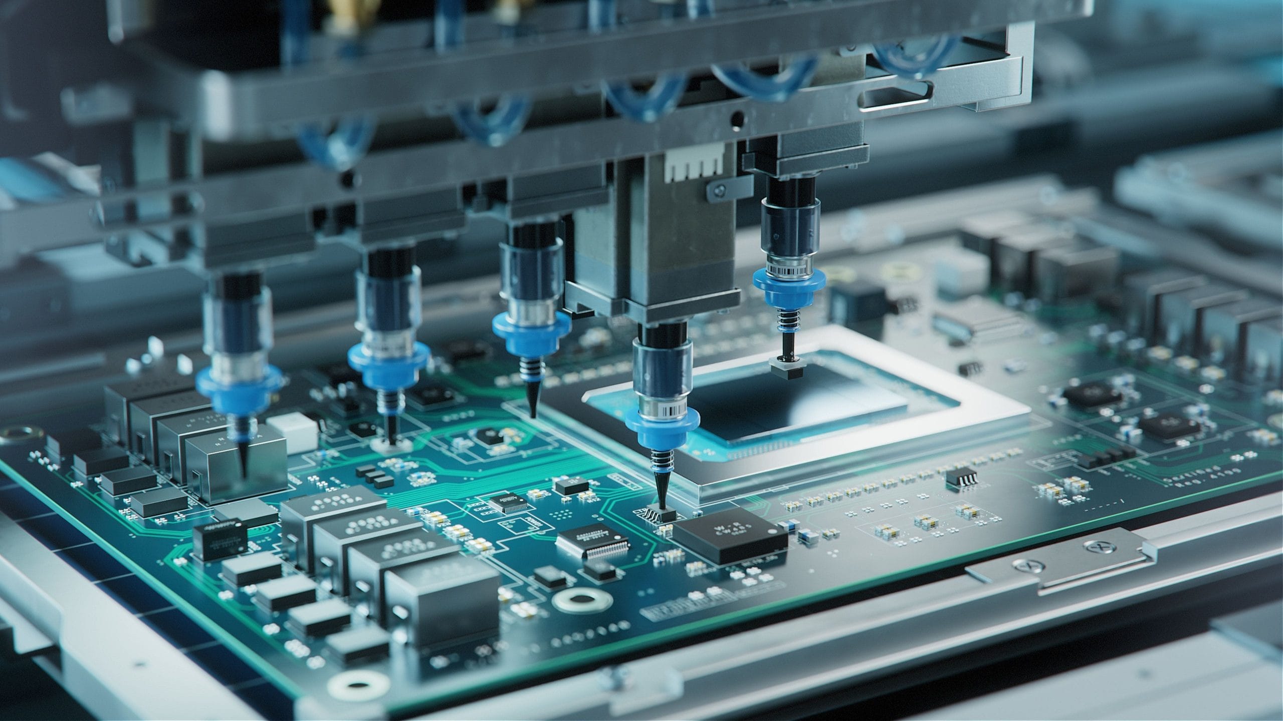
This comprehensive PCB assembly guide covers essential manufacturing standards[cite: 21]. Printed circuit board (PCB) assembly involves mounting electronic components onto a bare PCB to create a functional circuit[cite: 21]. Furthermore, this process encompasses placement, soldering, inspection, and testing[cite: 21]. Consequently, it transforms a blank board into the core of modern electronics[cite: 21].
Engineers typically perform PCB assembly using two primary methods[cite: 21]. These approaches are surface-mount technology and through-hole technology[cite: 21].
Surface-mount technology (SMT) attaches surface-mount devices (SMDs) directly onto PCB pads[cite: 21]. Afterwards, a controlled thermal reflow creates secure solder joints[cite: 21]. In contrast, through-hole technology (THT) inserts component leads into pre-drilled holes[cite: 21]. Soldering these leads on the opposite side forms robust mechanical connections[cite: 21].
In this PCB assembly guide, you will learn when to choose SMT versus THT[cite: 21]. Additionally, we explore specialized PCB assembly services[cite: 21]. These include potting, conformal coating, and low-pressure overmoulding to protect hardware in harsh environments[cite: 21].
Finally, you will discover how a contract manufacturing partner streamlines production[cite: 21]. We also outline key criteria for selecting an electronics manufacturing services provider[cite: 21].
Surface-mount technology in this PCB assembly guide
Surface-mount technology has modernized electronics manufacturing significantly[cite: 21]. Specifically, it attaches components directly to the PCB surface without drilled holes[cite: 21]. SMT components are smaller than through-hole parts[cite: 21]. Furthermore, they use metal terminations instead of wire leads to form soldered connections[cite: 21].
First, automated printers apply solder paste onto PCB pads[cite: 21]. Next, pick-and-place machines deposit each SMD accurately[cite: 21]. Finally, reflow ovens solder the components using a controlled thermal profile[cite: 21].
Although THT predates SMT, through-hole assembly remains indispensable[cite: 21]. This is because it provides superior mechanical strength[cite: 21]. Component leads pass through plated holes, and technicians apply solder on the opposite side[cite: 21]. Therefore, this method forms strong joints[cite: 21]. Consequently, engineers favor THT for connectors, large capacitors, and heavy mechanical loads[cite: 21].
Surface-mount technology vs. through-hole technology
SMT excels in miniaturization and high-volume throughput[cite: 21]. By supporting double-sided placement, SMT maximizes board density[cite: 21]. Therefore, it enables compact designs for consumer electronics[cite: 21].
Automated placement reduces manual labor and lowers unit costs during large runs[cite: 21]. However, initial capital expenditure for SMT machinery remains high[cite: 21]. Furthermore, small SMT solder joints offer less mechanical strength under severe stress without reinforcement[cite: 21].
Conversely, THT provides superior mechanical sturdiness[cite: 21]. Through-hole components withstand substantial axial forces[cite: 21]. Thus, THT suits applications where stress reliability is critical[cite: 21].
Additionally, this method simplifies prototyping and manual rework[cite: 21]. On the downside, THT consumes more board area[cite: 21]. As a result, it limits routing density and involves slower assembly, raising costs for large volumes[cite: 21].
Comparing SMT and THT: pros, cons and suitable applications
|
Technology |
Pros |
Cons |
Suitable applications |
|
SMT |
· Miniaturisation
· High density · Double-sided placement · Automated high volume · Lower per-unit cost at scale |
· High capital investment
· Less mechanical strength without reinforcement |
· Consumer electronics
· Mobile devices · Compact IoT modules |
|
THT |
· Superior mechanical robustness
· Easy prototyping & rework · Strong through-hole joints |
· Larger board footprint
· Labour-intensive · Higher cost per board at scale |
· Power supplies
· Industrial controls · Heavy-duty machinery or vehicles |
[cite: 21]
Key considerations for quality PCB assembly
Ensuring reliable manufacturing requires a complete strategy starting at the design phase[cite: 21].
Four critical pillars drive quality control: design for manufacturability (DFM), process inspection, environmental controls, and validation testing[cite: 21].
By integrating these practices into your workflow, you reduce rework significantly[cite: 21]. Furthermore, you accelerate time-to-market while achieving high yields[cite: 21].
Design for manufacturability (DFM)
Implementing DFM guidelines early in development reduces costs[cite: 21].
Essential DFM checks verify pad dimensions, solder clearances, and component spacing[cite: 21]. Specialized software tools automatically flag layout issues, enabling rapid iteration before fabrication[cite: 21].
Therefore, you should engage a manufacturing partner early[cite: 21]. This ensures your board layout aligns with supplier assembly tolerances[cite: 21].
Process controls and inspection
Consistent process controls are essential to ensure defect-free assembly[cite: 21]:
Material handling and the assembly environment
Proper material handling remains equally critical[cite: 21]. Staff must store moisture-sensitive components in humidity-controlled chambers[cite: 21]. Consequently, this prevents ‘popcorning’ defects during reflow[cite: 21]. Furthermore, maintaining ESD-protected areas prevents electrostatic discharge damage[cite: 21].
Additionally, technicians calibrate placement machines regularly[cite: 21]. This discipline maintains high placement accuracy and repeatability across builds[cite: 21].
Testing and validation
Post-assembly testing validates electrical performance before shipping[cite: 21].
Visual inspection catches surface flaws[cite: 21]. In-circuit testing verifies electrical connectivity[cite: 21]. Meanwhile, functional testing under operating conditions confirms overall performance[cite: 21]. Furthermore, incorporating boundary scan tests enhances coverage on complex boards[cite: 21].
The role of electronic contract manufacturing in PCB assembly
Outsourcing assembly to a specialist contract partner unlocks numerous advantages[cite: 21].
Contract manufacturers offer turnkey solutions covering sourcing, assembly, integration, and testing[cite: 21]. Furthermore, electronics manufacturing services provide after-market support and repairs[cite: 21]. This turnkey approach simplifies your supply chain significantly[cite: 21].
An integrated partner streamlines production, consolidates shipping, and maintains quality controls[cite: 21]. Consequently, this approach reduces lead times and lowers unit costs across production volumes[cite: 21].
Additionally, top providers offer advanced protection processes[cite: 21]. When hardware faces moisture, vibration, or chemical exposure, standard assembly alone may not suffice[cite: 21]. Therefore, complementary techniques—such as potting, conformal coating, and low-pressure overmoulding—ensure long-term durability[cite: 21].
Potting and encapsulation
Potting suits harsh-environment electronics, such as commercial transport systems, where long-term reliability is non-negotiable[cite: 21].
This process coats an assembled PCB with resin to seal components against moisture[cite: 21]. Robotic dispensing machines ensure precise compound ratios and void-free coverage[cite: 21].
Conformal coating
Conformal coating applies a thin polymer film over the PCB surface[cite: 21]. These coatings protect against dust and chemicals[cite: 21]. Consequently, they extend device service life[cite: 21].
Unlike potting, conformal coatings add minimal weight[cite: 21]. Therefore, they suit compact medical devices where space is constrained[cite: 21].
Low-pressure overmoulding and overmoulding
Low-pressure overmoulding injects hot-melt polyamides at low pressures to encapsulate boards[cite: 21]. Thus, it creates a protective barrier without damaging solder joints[cite: 21].
Meanwhile, traditional overmoulding embeds components into thermoplastics[cite: 21]. This process forms integrated housings for automotive sensors and industrial devices[cite: 21].
Partnering with an experienced contract specialist brings scalability and cost efficiencies[cite: 21]. When evaluating suppliers, select partners demonstrating strict process controls and certified standards[cite: 21].
Why choose EC Electronics for your PCB assembly services?
As a leading UK provider, EC Electronics brings 40 years of experience assembling high-quality PCB assemblies[cite: 21].
We deliver comprehensive PCB assembly services[cite: 21]. These range from flexible circuits to potting, encapsulation and conformal coating alongside low-pressure overmoulding[cite: 21].
Our modern facilities support both SMT and THT workflows[cite: 21]. Consequently, we handle everything from rapid prototype builds to complex multi-technology boards[cite: 21].
Furthermore, EC Electronics sources premium components from trusted distributors like Microchip, ST, AVX, VISHAY, and Kemet[cite: 21]. Technicians store moisture-sensitive parts in climate-controlled chambers to preserve optimal performance[cite: 21].
We build strictly to IPC-A-610 Class 3 standards[cite: 21]. Additionally, our ATEX-certified quality system guarantees intrinsic safety compliance for explosive environments[cite: 21]. Advanced 3D AOI inspection verifies all circuit functionality[cite: 21].
Ultimately, as outlined in this PCB assembly guide, our tailored services satisfy your exact production requirements[cite: 21].
Contact EC Electronics today at +44 (0)1256 461894 or sales@ecelectronics.com to discuss your next project[cite: 21].